SiPro – Fully Automated Silicon Photonics Probe Measurement System
Accelerate R&D to production with precise, repeatable, and scalable photonic device characterization.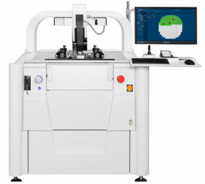
- End-to-end optical testing from wafer to module
- Integrated tunable laser and OSA with traceable calibration
- Recipe-based automation and report generation
Testing photonic devices shouldn’t be the bottleneck.
Manual probing and non-unified software create inconsistent results, slow wafer screening, and operator-dependent data. As silicon photonics moves into datacom, sensing, and biophotonics, labs and instrumentation centers need a standardized optical test platform.
SiPro delivers a fully automated measurement system that integrates precision mechanics, high-grade optical instruments, and intelligent software — so every engineer gets the same, traceable result.
Key advantages for R&D and production teams
Automation & Precision
7-DOF auto-alignment for sub-micron repeatability. Cuts alignment time by 5–10×.
Integrated Metrology
High-grade tunable laser and OSA with calibration documents suitable for metrology centers.
Smart Software
Unified interface for wavelength sweeps, data capture, and automated report generation. API available.
Scalable Platform
Start from semi-auto and upgrade to full-auto. Supports wafer-level and chip-level testing.
Integrated hardware and software architecture
SiPro combines all photonic test essentials into one platform:
- Optical source module (tunable laser)
- Optical analysis module (OSA)
- Probe & precision motion stage
- Control computer with measurement software
- Stable mechanical frame / enclosure
Every system ships with traceable instrument documentation, enabling reliable reporting for internal quality systems.
From wafer to report — in five steps
-
- Load wafer or chip on the stage
- Select measurement recipe from software
- Auto-align fibers or probe tips
- Run spectral sweep and capture data
- Export CSV/PDF or send to lab database
Built for advanced photonics programs
Applications
- Silicon photonics device characterization (e.g., grating couplers, MRRs, MZIs, and waveguides)
- Si and Si₃N₄ device testing
- Biosensing / mid-IR photonic chip validation
- Wafer-level screening in university or national labs
Industries
- Semiconductor / photonics foundries
- Photonics start-ups
- Research institutes & instrumentation centers
- Biomedical photonic chip developers
Technical highlights
| Wavelength range | 1250–1650 nm (custom options available) |
| Alignment accuracy | < 1 µm repeatability |
| Supported tests | Insertion loss, reflection, resonance, bandwidth, loss scan |
| Automation | 7-DOF alignment with software feedback |
| Data output | CSV, PDF report, real-time plots |
| Power / environment | 110–220 V, standard lab / cleanroom |
Request a demo or quotation
Tell us your chip type, wavelength range, and automation level. Our engineering team will propose the matching SiPro configuration.